Showing posts with label MICROCONTROLLER BASED PROJECTS. Show all posts

Feb 17, 2013

CONTROLLING WATER PUMP MACHINE USING CELLPHONE

INTRODUCTION

IN our country we face a common trouble of water although we badly need water supply for various purposes. In the buildings containing water roof tank and water pump for pumping water from any kind of ground level water source into the water roof tank, we can easily control the water pump machine in a very cheap and easy process. This project is more suitable in the buildings which have several levels containing many water taps, latrine water flashes, bath showers and water-heaters etc.
 
Some times we fall in trable when water supply is disrupted because of empty water tank. Then by calling
through a mobile phone to a phone number we can start the water pump motor and also can stop it when the water roof tank becomes fulfill.


Feb 16, 2013

HOME AUTOMATION OVER INTERNET

Stuff added in the project

  • Added Indicator for new message
  • Added New command to control dimness of LED
  • Updated Schematic
  • Updated Power Supply


AUTOMATIC PLANT IRRIGATION

Description

The Project presented here waters your plants regularly when you are out for vocation. The circuit comprises sensor parts built using op-amp IC LM324. Op-amp’s are configured here as a comparator. Two stiff copper wires are inserted in the soil to sense the whether the Soil is wet or dry. The
Microcontroller was used to control the whole system it monitors the sensors and when more than two sensors sense the dry condition then the microcontroller will switch on the motor and it will switch off the motor when all the sensors are in wet. The microcontroller does the above job it receives the signals from the sensors, and this signals operated under the control of software which is stored in ROM.


ACCIDENT ALERT AND VEHICLE TRACKING SYSTEM

This project is an intelligent Accident alert system which not only notifies accidental alert but also provides the exact location where the accident has taken place.  This project is basically built around the powerful ARM7 microcontroller by NXP LPC2148. A 3-axis accelerometer MMA8451Q connected over I2C bus is used detect the accident condition. On detection, ARM reads the current coordinates from the GPS module (MT3318 connected on uart) and send an SMS to a predefined number or a call center though SIM900 GSM modem. This sms carries location information so a quick help can be sent to save the victims.

Following is a quite explanatory video which shows the working model of the project. I am sure there are no more words needed to explain this project after seeing this video.


COMBINATION LOCK PROJECT WITH KEYPAD AND LCD

A Brief Description:

This project is written in C language. The basic user lock is of 2 Digits. The input is taken from a 4x3 Keypad (please see the schematic for more information) and Display the user input on a 2x16 LCD. A pin is assigned as output for activating and deactivating the lock. For demonstration I have connected an LED to that pin.

How combination lock works:

1. Turn switch on (5V DC voltage power supply)
2. A message name “Combination Lock” will display on LCD at first row,
3. Second row display “Enter Pass:” it asked you to enter password for open doors.
4. In this lock design it has three doors. These are the code locks to open doors “door1=05, door2=28, door3=82, door1 & door2 = 33”.
5. If you entered one of the codes in step 4 then press enter key that door will open. For example, you enter 05 for door 1 it’s then open and close door 1 after 5 seconds.
6. If codes you entered are not matched one of the code in step 4 then led door is not turn on.
7. If your first attempt failed the message “invalid code’ display on screen.
8. Then you pressed any key to clear and you can try for second attempt.

After you have reached three attempts but you have not entered correct password. Next Any Keys press alarm will activate for 5 seconds.


Using the Keypad:

Keypad has 12 keys (4x3) starting from 1,2,3,4,5,6,7,8,9,*,0,# (please see the schematic for layout). Numeric keys are used for entering numbers. '*' is used as the Cancel key and '#' is used as the Enter key.

Download File Information:

Flowchart.jpg
Combination_lock.c
Diagram bitmap.bmp
Lock_EBES_MODEL.DSN ( Using Proteus to run this file)
Combination_Lock.hex

Feb 14, 2013

INTERFACING DC MOTOR TO 8051

This article shows how to interface a DC motor to an 8051 microcontroller. Interfacing DC motor to 8051 forms an essential part in designing embedded robotic projects. A well designed 8051-DC motor  system  has essentially two parts. Firstly an 8051 with the required software to control the motor and secondly a suitable driver circuit. Most of the DC motors have  power requirements well out of the reach of a microcontroller and more over the voltage spikes produced while reversing the direction of rotation could easily damage the microcontroller. So it is not wise to connect a DC motor directly to the microcontroller. The perfect solution is to use a motor driver circuit in between the microcontroller and the DC motor.

L293 motor driver.

L293 is a dedicated quadruple half H bridge motor driver IC available in 16 pin package. To know more about H bridge, check this link. H bridge motor driver circuit . L293 has a current capacity of  600mA/channel and has supply voltage range from 4.5 to 36V DC. They are fitted with internal high speed clamp diodes for inductive spike protection. Other good features of L293 are high noise immunity, internal ESD protection, thermal shutdown, separate input supply for each channel etc. The pinout and truth table of an L293 motor driver is shown in the figure below.

 
L293 pinout and function diagram

Bi directional DC motor using 8051.

This project describes a bidirectional DC motor that changes its direction automatically after a preset amount of time  (around 1S).  AT89S51 is the microcontroller used here and L293 forms the motor driver. Circuit diagram is shown below.

 
Bi directional DC motor using 8051


In the circuit components R1, S1 and C3 forms a debouncing reset circuitry. C1, C2 and X1 are related to the oscillator. Port pins P1.0 and P1.1 are connected to the corresponding input pins of the L293 motor driver. The motor is connected across output pins 3 and 6 of the L293. The software is so written that the logic combinations of  P1.0 and P1.1 controls the direction of the motor. Initially when power is switched ON, P1.0 will be high and P1.1 will be low. This condition is maintained for a preset amount of time (around 1S) and for this time the motor will be running in the clockwise direction (refer the function table of L293). Then the logic of P1.0 and P1.1 are swapped and this condition is also maintained for the same duration . This makes the  motor to run  in the anti clockwise direction for the same duration and the entire cycle is repeated.

Program.

ORG 00H // initial starting address
MAIN: MOV P1,#00000001B // motor runs clockwise
ACALL DELAY // calls the 1S DELAY
MOV P1,#00000010B // motor runs anti clockwise
ACALL DELAY // calls the 1S DELAY
SJMP MAIN // jumps to label MAIN for repaeting the cycle
DELAY: MOV R4,#0FH
WAIT1: MOV R3,#00H
WAIT2: MOV R2,#00H
WAIT3: DJNZ R2,WAIT3
DJNZ R3,WAIT2
DJNZ R4,WAIT1
RET
END

Bidirectional motor with pushbutton control.

The circuit shown below is of an 8051 based  bi directional motor  whose direction can be controlled using 2 push button switches. The circuit is very similar to the previous one except  for the  two push button switches . These pushbutton switches are interfaced to  P0rt 3 of the microcontroller. Resistors R2 and R3 are the pull down resistors for P3.0 and 3.1 respectively.

 
Push button controlled bi-directional DC motor
 The code for the above project is so written that initially when power is switched ON, the motor remains OFF. When push button switch S2 is pressed P1.0 goes high and P1.1 remains low. The motor runs in the clockwise direction and this condition is maintained until S3 is pressed. When push button switch S3 is pressed the logic of P1.0 and P1.1 toggles making the motor to run in the opposite direction and this condition is maintained until the next press of S2.

Program.

ORG 00H // initiall starting address
MOV P3,#00000000B // initiates P3 as the pushbutton interface
MOV P1,#00000000B // clears P1 for keeping the motor OFF initially

MAIN:MOV A,P3 // moves the current state of P3 to Accumulator
CJNE A,#00000001B,LABEL1 // checks whether S2 is pressed
MOV P1,#00000001B // makes the motor run clockwise
LABEL1:CJNE A,#00000010B,LABEL2 // checks whether S3 is pressed
MOV P1,#00000010B // makes the motor to run anti clockwise
LABEL2:SJMP MAIN // jumps back to the MAIN loop
END

About the program.

Checking whether a particular push button is pressed is done using the CJNE (compare and jump if not equal) instruction. In simple words the CJNE instuction compares two operands and jump to a predefined LABEL  if the operands are not equal. If the two operands are equal nothing happens and the next instruction is executed.  Whenever push button S2 is pressed the status of P3 will be 00000001B .This status is moved to accumulator A and compared with 00000001B using the CJNE instruction. Both operands are equal means S2 is pressed and the next instruction (MOV P1,#00000001B) which makes the motor run clockwise is executed. If the operands are not equal that means the S2 is not pressed and the controller jumps to LABEL1 which is to check the S3. To check S3, status of P3 is moved to A again  and it is compared with 00000010B using the CJNE instruction. Both operands are equal means the S3 is pressed and the next instruction (MOV P1,#00000010B) which makes the motor run anti clockwise is executed. Both operands are not equal means S3 is not pressed and the controller goes to check  S2 again and this cycle is repeated.

Notes.

The maximum current capacity of L293 is 600mA/channel. So do not use a motor that consumes more than that.
The supply voltage range of L293 is between 4.5 and 36V DC. So you can use a motor falling in that range.

INTERFACING LCD WITH 8051

LCD display is an inevitable part in almost all embedded projects and this article is about  interfacing 16×2 LCD with 8051 microcontroller. Many guys find it hard to interface LCD module with the 8051 but the fact is that if you learn it properly, its a very easy job and by knowing it you can easily design embedded projects like digital voltmeter / ammeter, digital clock, home automation displays, status indicator display, digital code locks, digital speedometer/ odometer, display for music players etc etc. Thoroughly going through this article will make you able to display any text (including the extended characters) on any part of the 16×2 display screen. In order to understand the interfacing first you have to know about the 16×2 LCD module.

16×2 LCD module.

16×2 LCD module is a very common type of LCD module that is used in 8051 based embedded projects. It consists of 16 rows and 2 columns of 5×7 or 5×8 LCD dot matrices. The module were are talking about here is type number JHD162A which is a very popular one . It is available in a 16 pin package with back light ,contrast adjustment function and each dot matrix has 5×8 dot resolution. The pin numbers, their name and corresponding functions are shown in the table  below.


VEE pin is meant for adjusting the contrast of the LCD display and the contrast can be adjusted by varying the voltage at this pin. This is done by connecting one end of a POT to the Vcc (5V), other end to the Ground and connecting the center terminal (wiper) of of the POT to the VEE pin. See the circuit diagram for better understanding.
The JHD162A has two built in registers namely data register and command register.  Data register is for placing the data to be displayed , and the command register is to place the commands. The 16×2 LCD module has a set of commands each meant for doing a particular job with the display. We will discuss in detail about the commands later. High logic at the RS pin will select the data register and  Low logic at the RS pin will select the command register. If we make the RS pin high and the put a data in the 8 bit data line (DB0 to DB7) , the LCD module will recognize it as a data to be displayed .  If we make RS pin low and put a data on the data line, the module will recognize it as a command.
R/W pin is meant for selecting between read and write modes. High level at this pin enables read mode and low level at this pin enables write mode.
E pin is for enabling the module. A high to low transition at this pin will enable the module.
DB0 to DB7 are the data pins. The data to be displayed and the command  instructions are  placed on these pins.
LED+ is the anode of the back light LED and this pin must be connected to Vcc through a suitable series current limiting resistor. LED- is the cathode of the back light LED and this pin must be connected to ground.

16×2 LCD module commands.

16×2 LCD module has a set of preset command instructions. Each command will make the module to do a particular task. The commonly used commands and their function are given in  the  table below.


LCD initialization.

 The steps that has to be done for initializing the LCD display is given below and these steps are common for almost all applications.
  • Send 38H to the 8 bit data line for initialization
  • Send 0FH for making LCD ON, cursor ON and cursor blinking ON.
  • Send 06H for incrementing cursor position.
  • Send 01H for clearing the display and return the cursor.

Sending data to the LCD.

The steps for sending data to the LCD module is given below. I have already said that the LCD module has pins namely RS, R/W and E. It is the logic state of these pins that make the module to determine whether a given data input  is a command or data to be displayed.
  • Make R/W low.
  • Make RS=0 if data byte is a command and make RS=1 if the data byte is a data to be displayed.
  • Place data byte on the data register.
  • Pulse E from high to low.
  • Repeat above steps for sending another data.

Circuit diagram.

Interfacing 16x2 LCD module to 8051


The circuit diagram given above shows how to interface a 16×2 LCD module with AT89S1 microcontroller. Capacitor C3, resistor R3 and push button switch S1 forms the reset circuitry. Ceramic capacitors C1,C2 and crystal X1 is related to the clock circuitry which produces the system clock frequency. P1.0 to P1.7 pins of the microcontroller is connected to the DB0 to DB7 pins of the module respectively and through this route the data goes to the LCD module.  P3.3, P3.4 and P3.5 are connected to the E, R/W, RS pins of the microcontroller and through this route the control signals are transffered to the LCD module. Resistor R1 limits the current through the back light LED and so do the back light intensity. POT R2 is used for adjusting the contrast of the display.

Program.

MOV A,#38H // Use 2 lines and 5x7 matrix
ACALL CMND
MOV A,#0FH // LCD ON, cursor ON, cursor blinking ON
ACALL CMND
MOV A,#01H //Clear screen
ACALL CMND
MOV A,#06H //Increment cursor
ACALL CMND
MOV A,#82H //Cursor line one , position 2
ACALL CMND
MOV A,#3CH //Activate second line
ACALL CMND
MOV A,#49D
ACALL DISP
MOV A,#54D
ACALL DISP
MOV A,#88D
ACALL DISP
MOV A,#50D
ACALL DISP
MOV A,#32D
ACALL DISP
MOV A,#76D
ACALL DISP
MOV A,#67D
ACALL DISP
MOV A,#68D
ACALL DISP

MOV A,#0C1H //Jump to second line, position 1
ACALL CMND
MOV A,#67D
ACALL DISP
MOV A,#73D
ACALL DISP
MOV A,#82D
ACALL DISP
MOV A,#67D
ACALL DISP
MOV A,#85D
ACALL DISP
MOV A,#73D
ACALL DISP
MOV A,#84D
ACALL DISP
MOV A,#83D
ACALL DISP
MOV A,#84D
ACALL DISP
MOV A,#79D
ACALL DISP
MOV A,#68D
ACALL DISP
MOV A,#65D
ACALL DISP
MOV A,#89D
ACALL DISP
HERE: SJMP HERE
CMND: MOV P1,A
CLR P3.5
CLR P3.4
SETB P3.3
CLR P3.3
ACALL DELY
RET;
DISP:MOV P1,A
SETB P3.5
CLR P3.4
SETB P3.3
CLR P3.3
ACALL DELY
RET;
DELY: CLR P3.3
CLR P3.5
SETB P3.4
MOV P1,#0FFh
SETB P3.3
MOV A,P1
JB ACC.7,DELY
CLR P3.3
CLR P3.4
RET;
END

Subroutine CMND sets the logic of the RS, R/W, E pins of the LCD module so that the module recognizes the input data ( given to DB0 to DB7) as a command.
Subroutine DISP sets the logic of the RS, R/W, E pins of the module so that the module recognizes the input data as a data to be displayed .

INTERFACING SEVEN SEGMENT DISPLAY TO 8051

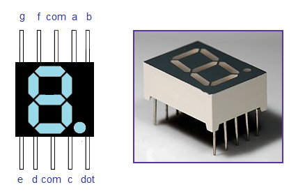
This article is about how to interface a seven segment LED display to an 8051 microcontroller. 7 segment LED display is  very popular and it can display digits from 0 to 9 and quite a few characters like A, b, C, ., H, E, e, F, n, o,t,u,y, etc. Knowledge about how to interface a seven segment display to a micro controller is very essential in designing embedded systems. A seven segment display consists of seven LEDs arranged in the form of a squarish ’8′ slightly inclined to the right and a single LED as the dot character. Different characters can be displayed by selectively glowing the required LED segments. Seven segment displays are of two types, common cathode and common anode. In common cathode type , the cathode of all LEDs are tied together to a single terminal which is usually labeled as ‘com‘   and the anode of all LEDs are left alone as individual pins labeled as a, b, c, d, e, f, g &  h (or dot) . In common anode type, the anode of all LEDs are tied together as a single terminal and cathodes are left alone as individual pins. The pin out scheme and picture of a typical 7 segment LED display is shown in the image below.

7 segment LED display

Digit drive pattern.

Digit drive pattern of a seven segment LED display is simply the different logic combinations of  its  terminals ‘a’ to ‘h‘ in order to display different digits and characters. The common digit drive patterns (0 to 9) of a seven segment display are shown in the table below.


Interfacing 7 segment display to 8051

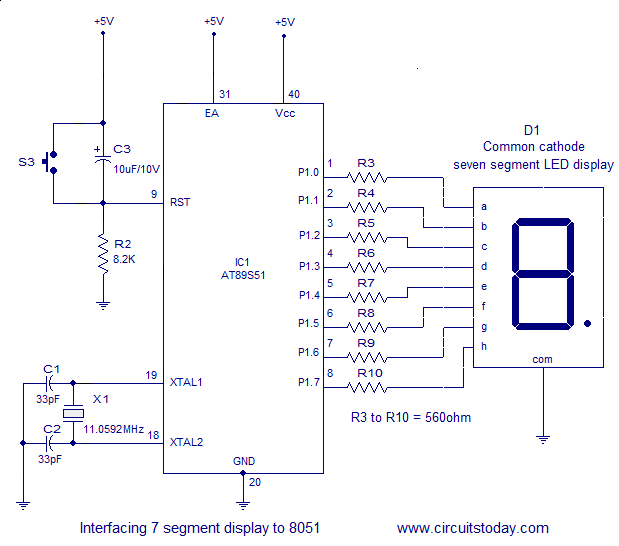
The circuit diagram shown above is of an AT89S51 microcontroller based 0 to 9 counter which has a 7 segment LED display interfaced to it in order to display the count.  This simple circuit illustrates two things. How to setup simple 0 to 9 up counter using 8051 and more importantly how to interface a seven segment LED display to  8051 in order to display a particular result. The common cathode seven segment display D1 is connected to the Port 1 of the microcontroller (AT89S51) as shown in the circuit diagram. R3 to R10 are current limiting resistors. S3 is the reset switch and R2,C3 forms a debouncing circuitry. C1, C2 and X1 are related to the clock circuit. The software part of the project has to do the following tasks.
  • Form a 0 to 9 counter with a predetermined delay (around 1/2 second here).
  • Convert the current count into digit drive pattern.
  • Put the current digit drive pattern into a port for displaying.
All the above said tasks are accomplished by the program given below.

Program.

ORG 000H //initial starting address
START: MOV A,#00001001B // initial value of accumulator
MOV B,A
MOV R0,#0AH //Register R0 initialized as counter which counts from 10 to 0
LABEL: MOV A,B
INC A
MOV B,A
MOVC A,@A+PC // adds the byte in A to the program counters address
MOV P1,A
ACALL DELAY // calls the delay of the timer
DEC R0//Counter R0 decremented by 1
MOV A,R0 // R0 moved to accumulator to check if it is zero in next instruction.
JZ START //Checks accumulator for zero and jumps to START. Done to check if counting has been finished.
SJMP LABEL
DB 3FH // digit drive pattern for 0
DB 06H // digit drive pattern for 1
DB 5BH // digit drive pattern for 2
DB 4FH // digit drive pattern for 3
DB 66H // digit drive pattern for 4
DB 6DH // digit drive pattern for 5
DB 7DH // digit drive pattern for 6
DB 07H // digit drive pattern for 7
DB 7FH // digit drive pattern for 8
DB 6FH // digit drive pattern for 9
DELAY: MOV R4,#05H // subroutine for delay
WAIT1: MOV R3,#00H
WAIT2: MOV R2,#00H
WAIT3: DJNZ R2,WAIT3
DJNZ R3,WAIT2
DJNZ R4,WAIT1
RET
END

About the program.

Instruction MOVC A,@A+PC is the instruction that  produces the required digit drive pattern for the display. Execution of this instruction will add the value in the accumulator A with the content of the program counter(address of the next instruction) and will move the data present in the resultant address to A. After this the program resumes from the line after MOVC A,@A+PC.
In the program,  initial value in A is 00001001B. Execution of  MOVC A,@A+PC  will add oooo1001B to the content  in PC ( address of next instruction). The result  will be the address of command DB 3FH (line15) and the data present in this address ie 3FH (digit drive pattern for 0) gets moved into the accumulator. Moving this pattern in the accumulator to Port 1 will display 0 which is the first count.
At the next count, value in A will advance to 00001010 and after the execution of  MOVC A,@+PC  ,the value in A will be 06H which is the digit drive pattern for 1 and this will display 1 which is the next count  and this cycle gets repeated for subsequent counts.
The reason why accumulator is loaded with 00001001B (9 in decimal) initially  is that the instructions from line 9 to line 15 consumes 9 bytes in total.
The lines 15 to 24 in the program which starts with command DB can be called as a Look Up Table (LUT). Command DB is known as Define Byte – which defines a byte. This table defines the digit drive patterns for 7 segment display as bytes (in hex format). MOVC operator fetches the byte from this table based on the result of adding PC and contents in the accumulator.
Register B is used as a temporary storage of the initial value of the accumulator and the subsequent increments made to accumulator to fetch each digit drive pattern one by one from the look up table(LUT).
Note:- In line 6, Accumulator is incremented by 1 each time (each loop iteration) to select the next digit drive pattern. Since MOVC operator uses the value in A to fetch the digit drive pattern from LUT, value in ACC has to be incremented/manipulated accordingly. The digit drive patterns are arranged consecutively in LUT.
Register R0 is used as a counter  which counts from 10 down to 0. This ensures that digits from o to 9 are continuously displayed in the 7 segment LED. You may note lines 4, 11, 12, and 13 in the above program. Line 4 initializes R0 to 10 (OAh). When the program counter reaches line 11 for the first time, 7 segment LED has already displayed 0. So we can reduce one count and that is why we have written DEC Ro. We need to continuously check if R0 has reached full count (that is 0). In order to do that lines 12 and 13 are used. We move R0 to accumulator and then use the Jump if Zero (JZ) instruction to check if accumulator has reached zero. If Acc=0, then we makes the program to jump to START (initial state) and hence we restart the 7 segment LED to display from 0 to 9 again. If Acc not equal to zero, we continue the program to display the next digit (check line 14).

Interfacing Seven segment display to 8051

A Note about 7 segment LED display.

This article is about how to interface a seven segment LED display to an 8051 microcontroller. 7 segment LED display is  very popular and it can display digits from 0 to 9 and quite a few characters like A, b, C, ., H, E, e, F, n, o,t,u,y, etc. Knowledge about how to interface a seven segment display to a micro controller is very essential in designing embedded systems. A seven segment display consists of seven LEDs arranged in the form of a squarish ’8′ slightly inclined to the right and a single LED as the dot character. Different characters can be displayed by selectively glowing the required LED segments. Seven segment displays are of two types, common cathode and common anode. In common cathode type , the cathode of all LEDs are tied together to a single terminal which is usually labeled as ‘com‘   and the anode of all LEDs are left alone as individual pins labeled as a, b, c, d, e, f, g &  h (or dot) . In common anode type, the anode of all LEDs are tied together as a single terminal and cathodes are left alone as individual pins. The pin out scheme and picture of a typical 7 segment LED display is shown in the image below.
seven segment LED display
7 segment LED display

Digit drive pattern.

Digit drive pattern of a seven segment LED display is simply the different logic combinations of  its  terminals ‘a’ to ‘h‘ in order to display different digits and characters. The common digit drive patterns (0 to 9) of a seven segment display are shown in the table below.
Digit a b c d e f g
0 1 1 1 1 1 1 0
1 0 1 1 0 0 0 0
2 1 1 0 1 1 0 1
3 1 1 1 1 0 0 1
4 0 1 1 0 0 1 1
5 1 0 1 1 0 1 1
6 1 0 1 1 1 1 1
7 1 1 1 0 0 0 0
8 1 1 1 1 1 1 1
9 1 1 1 1 0 1 1

Interfacing seven segment display to 8051.

interfacing 7 segment display to Atmel AT89S51
Interfacing 7 segment display to 8051
The circuit diagram shown above is of an AT89S51 microcontroller based 0 to 9 counter which has a 7 segment LED display interfaced to it in order to display the count.  This simple circuit illustrates two things. How to setup simple 0 to 9 up counter using 8051 and more importantly how to interface a seven segment LED display to  8051 in order to display a particular result. The common cathode seven segment display D1 is connected to the Port 1 of the microcontroller (AT89S51) as shown in the circuit diagram. R3 to R10 are current limiting resistors. S3 is the reset switch and R2,C3 forms a debouncing circuitry. C1, C2 and X1 are related to the clock circuit. The software part of the project has to do the following tasks.
  • Form a 0 to 9 counter with a predetermined delay (around 1/2 second here).
  • Convert the current count into digit drive pattern.
  • Put the current digit drive pattern into a port for displaying.
All the above said tasks are accomplished by the program given below.

Program.

ORG 000H //initial starting address
START: MOV A,#00001001B // initial value of accumulator
MOV B,A
MOV R0,#0AH //Register R0 initialized as counter which counts from 10 to 0
LABEL: MOV A,B
INC A
MOV B,A
MOVC A,@A+PC // adds the byte in A to the program counters address
MOV P1,A
ACALL DELAY // calls the delay of the timer
DEC R0//Counter R0 decremented by 1
MOV A,R0 // R0 moved to accumulator to check if it is zero in next instruction.
JZ START //Checks accumulator for zero and jumps to START. Done to check if counting has been finished.
SJMP LABEL
DB 3FH // digit drive pattern for 0
DB 06H // digit drive pattern for 1
DB 5BH // digit drive pattern for 2
DB 4FH // digit drive pattern for 3
DB 66H // digit drive pattern for 4
DB 6DH // digit drive pattern for 5
DB 7DH // digit drive pattern for 6
DB 07H // digit drive pattern for 7
DB 7FH // digit drive pattern for 8
DB 6FH // digit drive pattern for 9
DELAY: MOV R4,#05H // subroutine for delay
WAIT1: MOV R3,#00H
WAIT2: MOV R2,#00H
WAIT3: DJNZ R2,WAIT3
DJNZ R3,WAIT2
DJNZ R4,WAIT1
RET
END

About the program.

Instruction MOVC A,@A+PC is the instruction that  produces the required digit drive pattern for the display. Execution of this instruction will add the value in the accumulator A with the content of the program counter(address of the next instruction) and will move the data present in the resultant address to A. After this the program resumes from the line after MOVC A,@A+PC.
In the program,  initial value in A is 00001001B. Execution of  MOVC A,@A+PC  will add oooo1001B to the content  in PC ( address of next instruction). The result  will be the address of command DB 3FH (line15) and the data present in this address ie 3FH (digit drive pattern for 0) gets moved into the accumulator. Moving this pattern in the accumulator to Port 1 will display 0 which is the first count.
At the next count, value in A will advance to 00001010 and after the execution of  MOVC A,@+PC  ,the value in A will be 06H which is the digit drive pattern for 1 and this will display 1 which is the next count  and this cycle gets repeated for subsequent counts.
The reason why accumulator is loaded with 00001001B (9 in decimal) initially  is that the instructions from line 9 to line 15 consumes 9 bytes in total.
The lines 15 to 24 in the program which starts with command DB can be called as a Look Up Table (LUT). Command DB is known as Define Byte – which defines a byte. This table defines the digit drive patterns for 7 segment display as bytes (in hex format). MOVC operator fetches the byte from this table based on the result of adding PC and contents in the accumulator.
Register B is used as a temporary storage of the initial value of the accumulator and the subsequent increments made to accumulator to fetch each digit drive pattern one by one from the look up table(LUT).
Note:- In line 6, Accumulator is incremented by 1 each time (each loop iteration) to select the next digit drive pattern. Since MOVC operator uses the value in A to fetch the digit drive pattern from LUT, value in ACC has to be incremented/manipulated accordingly. The digit drive patterns are arranged consecutively in LUT.
Register R0 is used as a counter  which counts from 10 down to 0. This ensures that digits from o to 9 are continuously displayed in the 7 segment LED. You may note lines 4, 11, 12, and 13 in the above program. Line 4 initializes R0 to 10 (OAh). When the program counter reaches line 11 for the first time, 7 segment LED has already displayed 0. So we can reduce one count and that is why we have written DEC Ro. We need to continuously check if R0 has reached full count (that is 0). In order to do that lines 12 and 13 are used. We move R0 to accumulator and then use the Jump if Zero (JZ) instruction to check if accumulator has reached zero. If Acc=0, then we makes the program to jump to START (initial state) and hence we restart the 7 segment LED to display from 0 to 9 again. If Acc not equal to zero, we continue the program to display the next digit (check line 14).

Multiplexing 7 segment display to 8051.

Suppose you need a three digit display connected to the 8051. Each 7 segment display have 8 pins and so a total amount of 24 pins are to the connected to the microcontroller and there will be only 8 pins left with the microcontroller for other input output applications. Also the maximum number of displays that can be connected to the 8051 is limited to 4 because 8051 has only 4 ports. More over three 3 displays will be ON always and this consumes a considerable amount of power. All these problems associated with the straight forward method can be solved by  multiplexing .
In multiplexing all displays are connected in parallel to one port and only one display is allowed to turn ON at a time, for a short period. This cycle is repeated for at a fast rate and due to the persistence of vision of human eye, all digits seems to glow. The main advantages of this method are
  • Fewer number of port pins are required .
  • Consumes less power.
  • More number of display units can be interfaced (maximum 24).
The circuit diagram for multiplexing 2 seven segment displays to the 8051 is shown below.

Multiplexing 7 segement display to 8051


When assembled and powered on, the circuit will display the number ’16′ and let us see how it is done. Initially the first display is activated by making  P3.0 high and then digit drive pattern for “1″ is loaded to  the Port 1. This will make the first display to show “1″. In the mean time P3.1 will be low and so do the second display will be OFF. This condition is maintained for around 1ms and then P3.0 is made low. Now both displays will be OFF. Then the second display is activated by making P3.1 high and then the digit drive pattern for “6″ is loaded to the port 1. This will make the second display to show “6″. In the mean time P3.0 will be low and so the second display will be OFF.  This condition is maintained for another 1ms and then port 3.1 is made low. This cycle is repeated and due to the persistence of vision you will feel it as “16″.
Transistor Q1 drives the first display (D1) and transistor Q2 drives the second display (D2). R11 and R12 are the base current limiting resistors of Q1 and Q2. The purpose of other components are explained in the first circuit.

Program.

ORG 000H // initial starting address
MOV P1,#00000000B // clears port 1
MOV R6,#1H // stores "1"
MOV R7,#6H // stores "6"
MOV P3,#00000000B // clears port 3
MOV DPTR,#LABEL1 // loads the adress of line 29 to DPTR
MAIN: MOV A,R6 // "1" is moved to accumulator
SETB P3.0 // activates 1st display
ACALL DISPLAY // calls the display sub routine for getting the pattern for "1"
MOV P1,A // moves the pattern for "1" into port 1
ACALL DELAY // calls the 1ms delay
CLR P3.0 // deactivates the 1st display
MOV A,R7 // "2" is moved to accumulator
SETB P3.1 // activates 2nd display
ACALL DISPLAY // calls the display sub routine for getting the pattern for "2"
MOV P1,A // moves the pattern for "2" into port 1
ACALL DELAY // calls the 1ms delay
CLR P3.1 // deactivates the 2nd display
SJMP MAIN // jumps back to main and cycle is repeated

DELAY: MOV R3,#02H
DEL1: MOV R2,#0FAH
DEL2: DJNZ R2,DEL2
DJNZ R3,DEL1
RET
DISPLAY: MOVC A,@A+DPTR // adds the byte in A to the address in DPTR and loads A with data present in the resultant address
RET
LABEL1:DB 3FH
DB 06H
DB 5BH
DB 4FH
DB 66H
DB 6DH
DB 7DH
DB 07H
DB 7FH
DB 6FH
END


Feb 12, 2013

GSM CONTROLLED ROBOT


we already had a great start of this year with PIC Industrial and Domestic Timer project but that is not all for this year I received one more project today from students of Terna Polytechnic College. The is named as "Cellphone operated Land Rover" but i call it GSM controlled robot small and simple. well you can give name of your choice. 

In the project the robot is controlled by a mobile phone that makes a call to the mobile phone attached to the robot. In the course of a call, if any button is pressed a tone corresponding to the button pressed is heard at the other end called ‘Dual Tone Multiple frequency’ (DTMF) tone. The robot receives these tones with help of phone stacked in the robot. The received tone is processed by the microcontroller with the help of DTMF decoder ic cm8870 . This ic sends a signals to the the motor driver ic l293d which derives the motor forward, reverse…etc. Project is built using AVR microcontroller the ATmega16.

Project is a very simple and a good starter for robotics lover. Project also comes with complete project report and PCB layout which makes it even more easier for you to quickly start working. Here is a working sample of this project, I'm sure you'll be impressed with this simple idea   


DOWNLOAD FILE 

Feb 5, 2013

PIC diode tester

This is a simple use of the PIC 16F84 about a diode tester.
Test procedure : We set «1» to PB0 and «0» to PB3. If diode is ok and opens, then at PA0 we have «1». If PA0 is «0», then the the diode has problem. With the program we manage what the PIC will do in each situation . If PA0 is «1», green led lights wich means that the diode is OK and if PA0 is «0» red led is lighting and the diode is problematic
Test continuous as follows: We give «0» at PB0 and «1» to PB3. If diode is OK and opens, then at PA0 is «1». If PA0 is «0», then diode has problem. If PA0 is «1», green led lights that means that diode is OK and if PA0 is «0» the red diode is lights that means the the diode is problematic.
Source Code

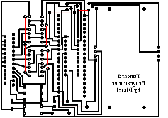
Funcard Programmer by Diesel

I have brought some modifications to the sideburn you monomake in the zip are included following files: Rame.bmp Rows in dimension originates them of the Componenti.bmp print Disposition of the members Ponti.bmp Disposition of the ponticelli to carry out .


Download in zip


Parts
R1-R2-R3 100 ohm
R4 470 ohm
D1 5,6 v diode zener
D2 diode led (attention to the polarity)
C1 4,7 , 16 v
IC1-IC2 74HC14 with relate hooves to you 14 pins
Smart Slot Smart Card
P1 Hoof 40 pins
P2 Hoof 20 pins (not sure to what it can serve?)
Connector 25 pins Male (parallel)
N.B. dimensions PCB 70,00 x 94,00 x 1,60 (milimeter), the resistances can be of greater values until 220(ohm), cos? like the condenser. I do not think responsible if something does not work, what fairies? to your risk and danger. To manufacture the programmer? lawyer to 100%. Usatelo for scopes only educated to you and without software that renders it illegal!!!!
Have FunCard!