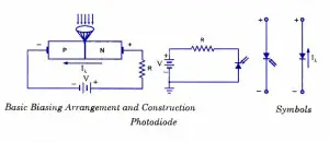
Photo-diode is a two-terminal semiconductor P-N junction
device and is designed to operate with reverse bias. The basic biasing
arrangement, construction and symbols for the device are given in
figure. It is either mounted in translucent case or has its
semiconductor junction mounted beneath an optical lens. The
output voltage is taken from across a series-connected load resistor
R. This resistance may be connected between the diode and ground or
between the diode and the positive terminal of the supply, as
illustrated in figure.
When
the P-N junction is reverse-biased, a reverse saturation current flows
due to thermally generated holes and electrons being swept across the
junction as the minority carriers. With the increase in temperature of
the junction more and more hole-electron pairs are created and so the
reverse saturation current I0 increases. The same effect can
be had by illuminating the junction. When light energy bombards a P-N
junction, it dislodges valence electrons. The more light striking the
junction the larger the reverse current in a diode. It is due to
generation of more and more charge carriers with the increase in level
of illumination. This is clearly shown in ‘ figure for different intensity levels. The dark current is
the current that exists when no light is incident. It is to be noted
here that current becomes zero only with a positive applied bias equals
to VQ. The almost equal spacing between the curves for the
same increment in luminous flux reveals that the reverse saturation
current I0 increases linearly with the luminous flux as shown
in figure. Increase in reverse voltage does not increase the reverse
current significantly, because all available charge carriers are already
being swept across the junction. For reducing the reverse saturation current I0
to zero, it is necessary to forward bias the junction by an amount
equal to barrier potential. Thus the photodiode can be used as a photoconductive device.
On
removal of reverse bias applied across the photodiode, minority charge
carriers continue to be swept across the junction while the diode is
illuminated. This has the effect of increasing the concentration of
holes in the P-side and that of electrons in the N-side But the barrier
potential is negative on the P-side and positive on the N-side, and was
created by holes flowing from P to N-side and electrons from N to P-side
during fabrication of junction. Thus the flow of minority carriers
tends to reduce the barrier potential.
When
an external circuit is connected across the diode terminals, the
minority carrier; return to the original side via the external circuit.
The electrons which crossed the
junction from P to N-side now flow out through the N-terminal and into
the P-terminal This means that the device is behaving as a voltage cell
with the N-side being the negative terminal and the P-side the positive
terminal. Thus, the photodiode is & photovoltaic device as well as
photoconductive device.
Photodiodes have a far lower light sensitivity than cadmium sulphide LDR s,
but giving a fair quicker response in light level. Generally LDRs are
ideal for use in slow acting direct coupled light-level sensing
applications, while photodiodes are ideal for use in fast acting ac
coupled signalling applications. Typical photodiode applications include
detection (both visible and invisible), demodulation, switching, logic
circuits that need stability and high speed, character recognition,
optical communication equipment, IR remote control circuits encoders etc.

No comments:
Post a Comment